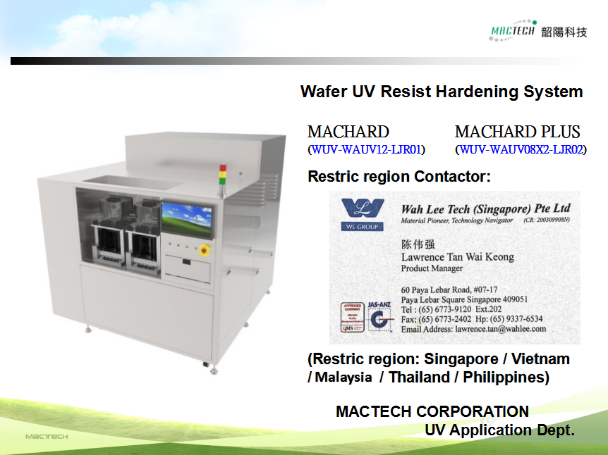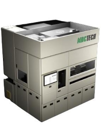
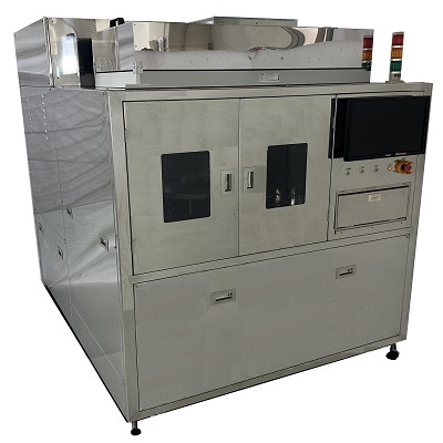
High-intensity ultraviolet irradiation increase throughput
2.Min. 300mW/cm²(at wavelengths 365 nm)
3.Wafer size:300/200/150mm
4.Incorporates facilities for measurement of spectral distribution,adjustment for 5levels of intensity,and integrated irradiation control.
5.Radiation distribution:Max. +-10%(measured at 5 points on a wafer in H mode)
6.Clean,fast wafer handling
7.Space-saving design
8.Complete safety design
|
ITEM |
Specification |
|
Wafer size |
Φ300/200/150mm |
|
M/C size (WxDxH) |
195 X 200 X 250 cm |
|
Power supply |
AC 380V/220V 50/60Hz 3 Φ |
|
Irradiance |
Min. 300mW/cm² (at wavelengths ranging from220 to 320nm) |
|
Max.hot plate temperature |
250℃ |
|
Hot-plate temperature rise rat |
T/△t=2.0±0.2℃/sec (△T≧150℃,H-mode) |
|
Wafer transfer mechanism |
Wafer robot(RWSE/RWDE) |
|
LOAD PORT |
Manual / Auto |
|
Method for setting process condition |
PC BASE MMI |
|
Program setting mode |
5 modes |
|
Certified |
SEMI S2(option) |
Main Application:
1.Enhancement of thermal resistance of photoresist and degassing from photoresist prior to ion implantation process
2.Erasure of electrical charge and removal of stress
3.This uv photoresist curing system employed in VLSI fabrication lines as UV irradiation equipment
Equipment Feature:
1.Less 5 minutes replacement lamp
2.User friendly operation by PC base
3.Possible to control intensity decreasing by build in intensity monitor. Periodic measurement at the center of stage
4.High productivity by High Intensity UV lamp